STEM IN STYLE SERIES: EPISODE III

You are most likely reading this on an electronic device that runs with multiple semiconductor devices. Apps, video chat, streaming are a few of the game-changing things only possible because of exponential growth in computing power. Increased demand for immense computing power on smaller and lighter devices, has driven companies like Intel and Samsung to innovate ingenious ways to fit more transistors onto computer chips. One of the key processes in such device fabrication is called chemical-mechanical planarization or CMP.
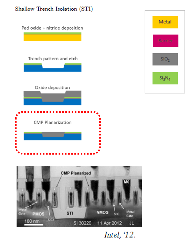
Chemical-mechanical planarization (CMP) is a process of smoothing surfaces with the combination of chemical and mechanical forces, and is key to semiconductor device integration. One major example of CMP process in device fabrication is in Shallow trench isolation (STI) processes. Shallow trench isolation is a process used to fabricate semiconductor devices that prevents electric current leakage between adjacent device components. This is key in increasing integrated circuit density on a chip. It involves etching a pattern of trenches in the silicon and then depositing an insulating material (dielectric) between the active areas. The excess dielectric material is removed by chemical mechanical planarization (CMP)!
Image courtesy Joy Johnson
CMP uses a colloidal solution that is both an abrasive and corrosive chemical slurry. The semiconductor wafer is placed face down on a wafer carrier and polished with the abrasive slurry on a pad as shown below. It is a remarkably effective process that can bring a wafer’s surface within the depth-of-field of a photo-lithography system.
Schematic of a chemical mechanical planarization setup (image courtesy Joy Johnson).
The major advantage of the CMP process is the unique ability to remove material in a planar and uniform fashion, consistently and to significantly tight process control requirements on multiple materials at once. In addition, throughput is quite decent as you can polish large wafers (>=300mm) in one process. However, the major limitation of this process are performance limiting defects and yield fallout as a result of ‘blind polishing.' It is difficult to determine if the desired amount of material will removed or the desired degree of planarization has reached in many processes without attempting multiple test runs or blinding extrapolating from similar demos. Thus, the cost, in both time and materials, associated with doing a prior DoE for a new device or material benefits greatly from modeling that helps to de-risk excursions due to agglomerates. In CMP, the formation of large agglomerates is of great concern, as these large particles are associated with high defect density and poor polishing performance.
Joy’s PhD work was to use an empirical (experimental) and theoretical approach to modelling the CMP process control and optimization.
Her work is the first fully integrated slurry agglomeration particle-level model. Some examples of questions her model can answer are:
How does mechanical shear affect abrasive particle agglomeration in a simple slurry system?
How is shear-induced agglomeration affected by pH/size?
How is shear-induced agglomeration affected by chemical additives?
Joy’s work is significantly crucial to CMP optimization and significant cost savings in semiconductor fabrication.


